CSP, 0201 passive components, lead-free soldering and optoelectronics are arguably the hottest technologies that many companies have recently practiced and positively evaluated on PCBs.
For example, how to deal with the ultra-small opening (250um) problem common in CSP and 0201 assembly is the basic physical problem that solder paste has never had before. Board-level optoelectronic assembly, as a major area of ​​communication and network technology development, is very elaborate. Typical packages are expensive and fragile, especially after device lead formation. The design guidelines for these complex technologies are also very different from the normal SMT process because board design plays a more important role in ensuring assembly productivity and product reliability;
For example, for CSP solder interconnects, reliability can be significantly improved simply by changing the board bond pad size.
CSP applications One of the key technologies that is common today is CSP. The appeal of CSP technology is that it has many advantages, such as reduced package size, increased pin count, enhanced performance, and reworkability of the package.
The high-efficiency advantages of CSP are as follows: for board-level assembly, it is possible to cross the fine-pitch (thin to 0.075 mm) perimeter package and enter a larger pitch (1, 0.8, 0.75, 0.5, 0.4 mm) area array structure. Many CSP devices have been used in the consumer telecom field for many years and are widely considered to be low cost solutions in the areas of SRAM and DRAM, medium pin ASIC, flash memory and microprocessor.
CSPs can have four basic characteristics: rigid base, flexible base, lead frame base, and wafer level scale.
CSP technology can replace SOIC and QFP devices as mainstream component technologies.
One problem with the CSP assembly process is that the bond pads of the solder interconnect are small. Usually, the bonding pad size of the 0.5 mm pitch CSP is 0.250 to 0.275 mm. With such a small size, it is difficult to print a solder paste through an opening having an area ratio of 0.6 or less. However, with a well-designed process, printing can be successfully performed.
The failure usually occurs due to insufficient solder due to clogging of the template opening. Board-level reliability depends mainly on the package type, while CSP devices can withstand an average thermal cycle of -400 to 1.25 °C for 800 to 1200 times, eliminating the need for underfill. However, the thermal reliability of most CSPs can be increased by 300% if underfill materials are used. CSP device failures are generally associated with solder fatigue cracking. Advances in Passive Components Another major emerging area is the 0201 passive component technology, which is of great interest to the 0201 component due to the market need to reduce board size. Since the introduction of 0201 components in mid-1999, cellular manufacturers have assembled them with CSPs, reducing the size of the plates by at least half. Handling such packages is quite cumbersome, and to reduce the occurrence of post-process defects such as bridging and erection, pad size optimization and component spacing are key. As long as the design is reasonable, these packages can be placed close to each other with a pitch as small as 150 μm.
In addition, the 0201 device can be placed under the BGA and the larger CSP.
A cross-sectional view of 0201 below the CSP assembly. Due to the small size of these small discrete components, assembly equipment manufacturers have planned to develop newer systems compatible with the 0201. Through-hole assembly still has vitality Optoelectronic packages are widely used in the telecommunications and networking fields where high-speed data transmission is prevalent. Ordinary board-level optoelectronic devices are "butterfly-shaped" modules. Typical leads for these devices extend from the sides of the package and expand horizontally. The assembly method is the same as that of the through-hole components, and is usually performed by a manual process in which the leads are processed by a lead forming pressure tool and inserted into the plate via holes through the substrate.
The main problem with handling such devices is the damage to the leads that can occur during the lead forming process. Since such packages are expensive, care must be taken to prevent the leads from being damaged by the molding operation or the module package being broken at the lead-device body connection. After all, the solution to incorporating optoelectronic components into standard SMT products is to use automated equipment so that components are removed from the disk and placed on the lead forming tool, after which the leaded device is removed from the molding machine. Then place the module on the plate. Given that this option requires considerable capital investment in equipment, most companies will continue to choose manual assembly processes.
Large format printers (20 x 24") are also common in many manufacturing applications. Products such as set-top boxes and routing/switching plates are quite complex, including a mix of the various techniques discussed herein, for example, in Large ceramic grid arrays (CCGA) and BGA devices up to 40 mm2 are often seen on this type of board.
The two main problems with such devices are the large heat dissipation and the warpage caused by heat. These components can act as large heat sinks, causing non-uniform heating under the package surface, which may result in non-wetting solder joints near the center of the device due to thermal control of the furnace and heating curve control. The warpage of the device and the printing plate caused by heat during processing may result in "non-wetting phenomenon" such as separation of the components from the solder paste applied to the printing plate. Therefore, care must be taken when mapping the heating curves of these plates to ensure uniform heating of the BGA/CCGA surface and the entire plate surface. Plate Warpage Factors To avoid excessive bending of the plate, it is important to properly support the plate in the reflow oven. Plate warpage is an important factor that must be observed in circuit assembly, and should be strictly described. BGA or substrate warpage caused by heat in the reflow cycle causes solder voids and leaves a large amount of residual stress on the solder joint, causing early failure. This type of warpage is easily described using a moiré fringe projection image system that can be operated online or offline to describe the pre-treatment package and plate warpage. The offline system can also simulate a reflow environment by using time/temperature coordinate based warp patterns set for the device and the plate in the furnace.
Lead-free soldering
Lead-free soldering is another new technology that many companies have begun to adopt. This technology began in the European Union and Japanese industries, initially to remove lead from solder during PCB assembly. The date of implementation of this technology has been changing, initially proposed in 2004, and Zui's recently proposed date was achieved in 2006. However, many companies are now striving to own the technology in 2004, and some companies now offer lead-free products.
There are many lead-free solder alloys on the market today, and an alloy composition commonly used in the US and Europe is 95.6Sn ∕ 3.7Ag ∕ 0.7Cu. There is not much difference in handling these solder alloys compared to standard Sn/Pb solders. The printing and placement processes are the same, the main difference being the reflow process, which means that higher liquidus temperatures must be used for most lead-free solders. The Sn∕Ag∕Cu alloy generally requires a peak temperature of about 30 ° C higher than that of the Sn/Pb solder. In addition, preliminary studies have shown that the reflow process window is much more stringent than standard Sn/Pb alloys. For small passive components, reducing surface energy also reduces the number of upright and bridging defects, especially for 0402 and 0201 size packages. In summary, the reliability of lead-free assembly indicates that it is comparable to Sn/Pb solder, except for high temperature environments, such as operating temperatures in automotive applications that may exceed 150 °C.
Flip film
When integrating current advanced technologies into standard SMT components, the technology encounters difficulties. In primary packaged component applications, flip-chips are widely used in BGA and CSP, although BGA and CSP have adopted lead-frame technology. In board-level assembly, the use of flip-chips offers many advantages, including reduced component size, improved performance, and reduced cost.
Unfortunately, the use of flip chip technology requires manufacturers to increase their investment in order to upgrade their machines and add specialized equipment for the flip chip process. These devices include placement systems and underfill dispensing systems that meet the high precision requirements of flip chip. In addition, X-ray and sound image systems are included for post-reflow solder joint inspection and post-fill cavity analysis. Pad designs, including shape, size, and mask definition, are critical to manufacturability and testability (DFM/T) and cost requirements.
On-board flip chip (FCOB) is mainly used in products that are critical to miniaturization, such as Bluetooth module components or medical device applications. Figure 4 shows a Bluetooth module board that incorporates flip chip technology in the same package as the 0201 passive component. The same high-speed placement and handling of flip-chip and 0201 devices can also place solder balls around the perimeter of the package. This can be said to be a good example of implementing advanced technology on standard SMT assembly lines.
Imported French lens
Mould Die-casting Eight edge type Revolving arm
Each LED can be replaced individually, which guarantees maximum economy.
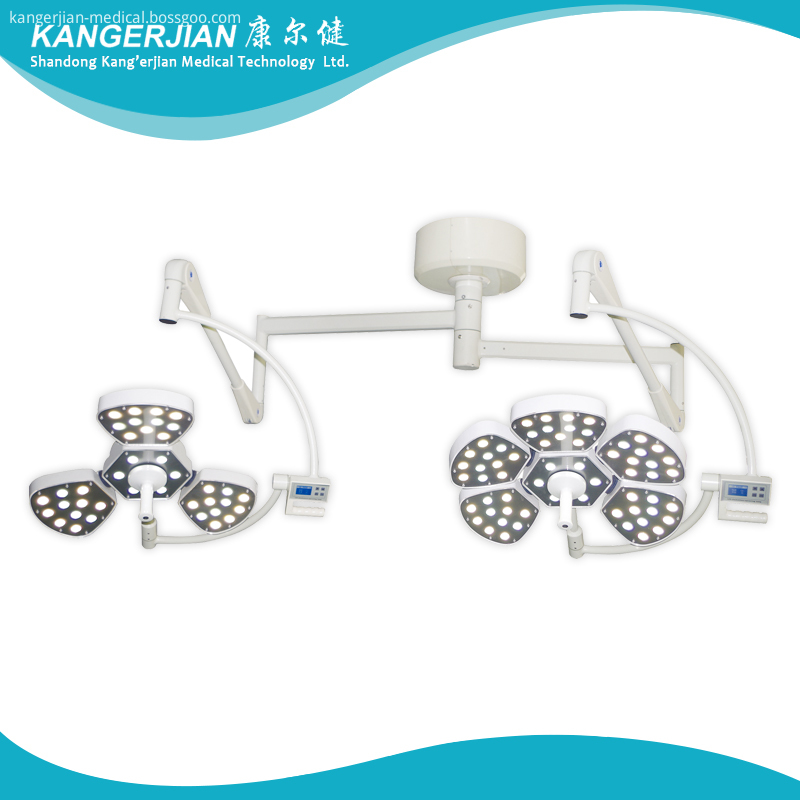
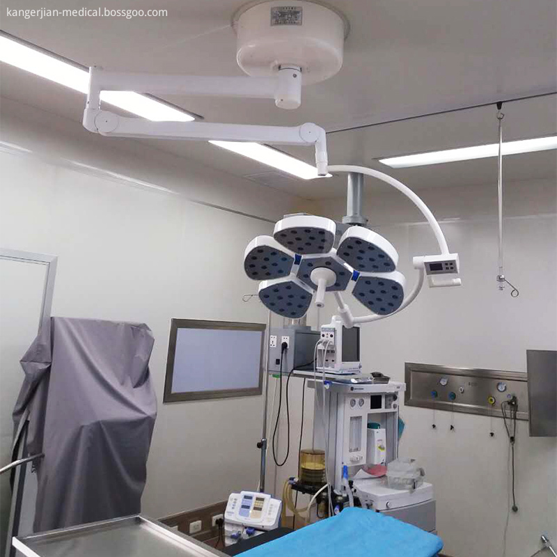
Configuring lightweight balance arm suspension system ,six groups universal joint linkage ,mobile, lightweight positioning and stablibity .A 360°all-round design ,can meet the need for surgery in different heights and angles.
Color temperature constant, soft, very close to the natural sun light.
The use of liquid crystal display button control, to meet the needs of the medical staff of different patients with the brightness of the operation.


Flower Type Operating Light,Operating Room Lights,Petal Led Surgical Lights,Petal Type Led Surgical Lights
Shandong qufu healthyou Medical Technology co.,Ltd , https://www.kangerjian-medical.com